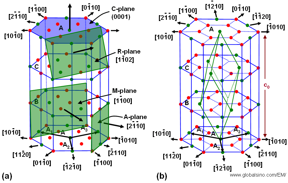
Sapphire Substrate Crystal Structure
Alpha A Alumina Sapphire

Coordinate System And Sapphire Crystal Geometry Showing The Spatial Download Scientific Diagram

Manufacturing And Supply Of Industrial Sapphire Monocrystal

A Coordinate Systems In The Sapphire Crystal And The R Plane And B Download Scientific Diagram
Sapphire Substrates Ossila

Figure 1 From Silicon On Sapphire Sos Device Technology Semantic Scholar

Substrate analysis sos structure.
Sapphire substrate crystal structure.

Schematic Presentation Of The Wurtzite Crystal Structure Of Group Iii Download Scientific Diagram

A Crystal Structure Of Al 2 O 3 0001 Where The Blue Balls Denotes Download Scientific Diagram

Sapphire Optical Material
Sapphire Substrate An Overview Sciencedirect Topics

Figure 1 From Copper Crystals On The 11 20 Sapphire Plane Orientation Relationships Triple Line Ridges And Interface Shape Equilibrium Semantic Scholar
New Page 1

Research On Ground Surface Characteristics Of Prism Plane Sapphire Under The Orthogonal Grinding Direction Sciencedirect

Pdf Modern Trends In Crystal Growth And New Applications Of Sapphire

Schematics Of The Atomic Arrangements For A Al 2 O 3 Lattice And The Download Scientific Diagram

Sapphire Crystal Meaning Crystal Meanings Crystals Crystal Therapy
Schematic For Gan Grown On Different Lattice Mismatched Substrates A Download Scientific Diagram
Ti Sapphire Crystals 4lasers

Machine Learning Application For Prediction Of Sapphire Crystals Defects Sciencedirect
The Devil Is In The Details Features Aug 2009 Photonics Spectra

Control Of Crystal Structure Of Ga2o3 On Sapphire Substrate By Introduction Of A Alxga1 X 2o3 Buffer Layer Jinno 2018 Physica Status Solidi B Wiley Online Library

Structural Morphological Optical And Electrical Properties Of Zn Sub 1 X Sub Cd Sub X Sub O Solid Solution Grown On I A I And I R I Plane Sapphire Substrate By Mocv

Material Removal Mechanism Of Sapphire Substrates With Four Crystal Orientations By Double Sided Planetary Grinding Sciencedirect
Https Encrypted Tbn0 Gstatic Com Images Q Tbn 3aand9gct5 Vw3jxirgvqzkzeke06e3ffzbqgxkoq3twhf2c2gsl 3lthz Usqp Cau
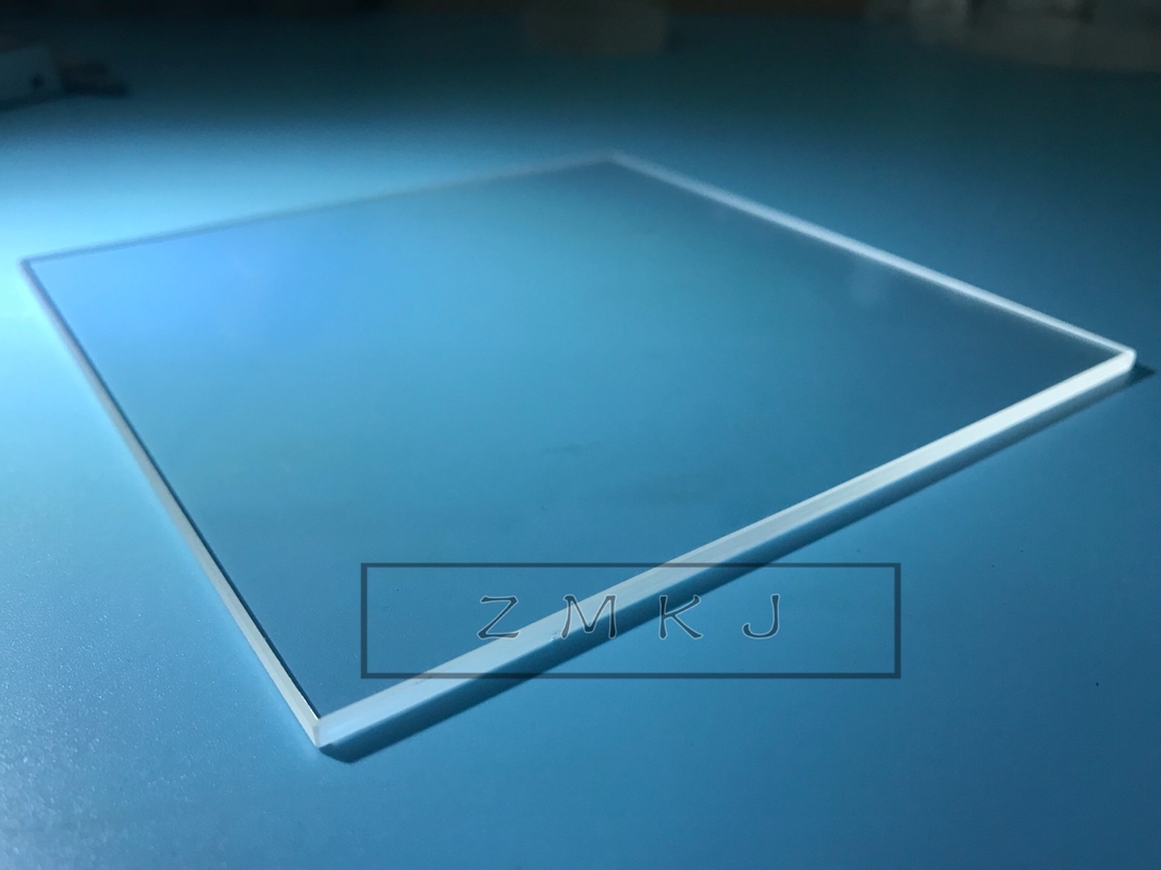
116x116mm Square Sapphire Optical Windows Sapphire Crystal Glass 8mm Thickness

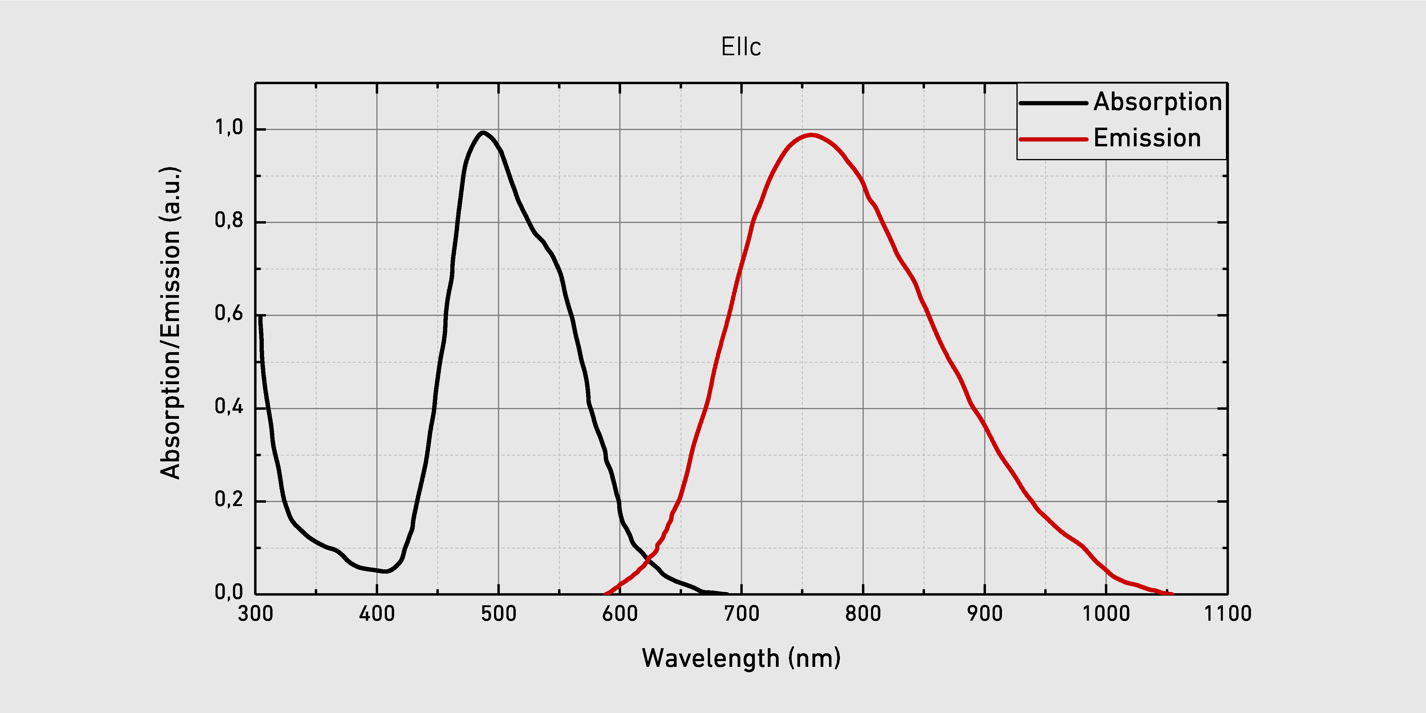
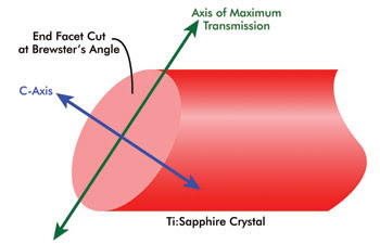
Ti Sapphire Crystals Sapphire Optics For Ultrafast Lasers Gtat

Pdf Properties Of Sapphire

Pin On Cmfe By Coherent

Surface Defects In Efg Sapphire Single Crystals Sciencedirect
Source : pinterest.com
